The lpGBT ASIC (Low Power GigaBit Transceiver) is a new 65nm-CMOS radiation tolerant serializer/deserializer device that can be used on the front-end electronics of the HL-LHC detectors. This component is foreseen to be used by CMS and ATLAS for their system upgrades and offers a set of encoding and decoding schemes specifically tailored to meet their needs in terms of radiation-hardness and data bandwidth.
The lpGBT-FPGA project started in 2018 as a natural evolution of the existing GBT-FPGA to provide a back-end counterpart to the future lpGBT ASIC. The new FPGA IP implements the encoding/decoding schemes supported by the front-end ASIC, meaning that it can be configured using 4 different combinations for the upstream link (from Front-end to Back-end): two decoding schemes (FEC5 or FEC12) based on Reed-Solomon techniques to configure the encoding robustness and two line rates (10.24 or 5.12Gbps) depending on the required bandwidth. Additionally, the lpGBT-FPGA core features an asymmetric architecture to match the lpGBT ASIC specificities: the transmitter part of the IP, as opposed to the configurable receiver part, proposes a single encoding scheme (FEC12) and a lower line rate of 2.56Gbps. Such an asymmetry prevents the IP to be used in loopback mode for self-testing.
Links
Core Repository architecture
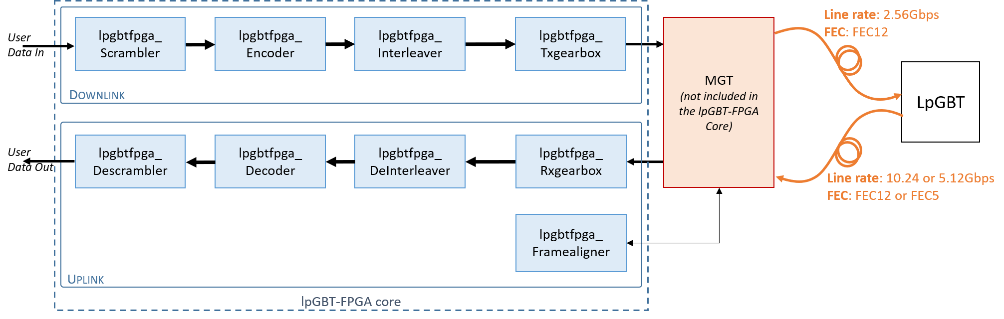
- lpGBT_FPGA_downlink: Contains the top files that interconnect the downstream datapath modules (encoder, scrambler, gearbox). This entity in not configurable, as there is one single line rate and FEC for the downlink path.
- lpGBT_FPGA_uplink: Contains the top files that interconnect the upstream datapath modules (frame aligner, gearbox, decoder, descrambler). This entity is configurable before implementation to select the line rate and the FEC type.
- Note that the MGT is not part of the lpGBT_FPGA core
Modules description
The lpGBT-FPGA provides a back-end counterpart to the lpGBT asic meaning that it implements the SerDes to deal with the high speed side (5.12Gbps or 10.24Gbps). Because of the range of available configurations, and in order to avoid having a too comprehensive and heavy IP to integrate, the uplink part of the lpGBT-FPGA core shall be configured by the user before implementation. No dynamic implementation is proposed from the 2.0.0 version any more. According to this philosophy, the lpGBT-FPGA core implemented by the user keeps really limited in terms of resource. The block diagram below shows the interconnections of the differents blocks available:
Downlink datapath
Architecture
The downlink datapath encodes the data according to the lpGBT specification, using a specific implementation of the reed-solomon encoder. The lpgbtfpga_downlink entity is made of 4 blocks:
- Scrambler
- Encoder
- Interleaver
- Tx gearbox
It is designed to operate at the transceiver user clock, typically at 320MHz, using a multicycle path architecture with a clock enable signal (with a 1 to 8 ratio). The example design contains an example of how the user can implement a clock-domain-crossing ensuring fixed-latency between a 40MHz clock and the core. The frame size is 64bit (including the FEC). It provides a user bandwidth of 1.28Gbps and 2 additional fields for the slow control of 80Mbps are also available. The total line rate is 2.56Gbps.
Downlink Frame
The downlink frame of the lpGBT-FPGA is made of:
- Header (4bit): Used by the lpGBT to align the frame.
- User data (32bit): sent to lpGBT e-links.
- EC (2bit): used for the external slow control (e.g.: GBT-SCA).
- IC (2bit): used for the internal slow control of the lpGBT (register configuration).
- FEC (24bit): used to recover from transmission error (can correct up to 12 consecutives errors).
Instantiation parameters:
The 3 generic parameters available for the lpgbtfpga_downlink entity are reserved for expert tuning (a recommended initialisation is proposed in the example designs projects):
c_multicyleDelay: is used to relax the timing constraints and is typically set to 3,c_clockRatio: is used to configure the gearbox, with respect to its output and input clocks (freq_out/40MHz). For 320MHz reference clock, the value is typically 8.c_outputWidth: corresponds to the MGT word size and shall be set up accordingly. This value is typically 32 bits.
Additional details about the module (ports, architecture ...) are available here
Uplink datapath
Architecture
The uplink datapath decodes the data, according to the lpGBT specification, using a specific implementation of reed-solomon decoders. The lpgbtfpga_uplink entity is made of 5 blocks:
- frame_aligner
- rx_gearbox
- deinterleaver
- decoder
- descrambler
It is designed to operate at the transceiver user clock, typically at 320MHz, using a multicycle path architecture with a clock enable signal (with a 1 to 8 ratio). The example design contains an example of how the user can implement a clock-domain-crossing ensuring fixed-latency between a 40MHz clock and the core.
Uplink frame
The user frame size is 128 or 256bit (including the FEC), depending on the datarate (10.24 or 5.12Gbps).
This path is configurable as follow:
- 5.12Gbps / FEC5:
- Header(2bit): Used by the lpGBT to align the frame.
- Slow control (4bit): IC (2bit) and EC (2bit).
- User bandwith (112bit): From lpGBT e-links.
- FEC (10bit): Can correct up to 5 consecutives errors.
- 5.12Gbps / FEC12:
- Header(2bit): Used by the lpGBT to align the frame.
- Slow control (4bit): IC (2bit) and EC (2bit).
- User bandwith (98bit): From lpGBT e-links (2bit unconnected).
- FEC (24bit): Can correct up to 5 consecutives errors.
- 10.24Gbps / FEC5:
- Header(2bit): Used by the lpGBT to align the frame.
- Slow control (4bit): IC (2bit) and EC (2bit).
- User bandwith (230bit): From lpGBT e-links (6bit unconnected).
- FEC (20bit): Can correct up to 5 consecutives errors.
- 10.24Gbps / FEC12:
- Header(2bit): Used by the lpGBT to align the frame.
- Slow control (4bit): IC (2bit) and EC (2bit).
- User bandwith (202bit): From lpGBT e-links (10bit unconnected).
- FEC (48bit): Can correct up to 5 consecutives errors.
Instantiation parameters:
Two important parameters allow the user to configure the uplink as described above (instantiation examples are proposed in the example designs projects):
- DATARATE: which can be set either to "DATARATE_10G24" or to "DATARATE_5G12"
- FEC: which can be set either to "FEC5" or to "FEC12"
Some generic parameters are additionally available for expert tuning (a recommended initialisation is proposed in the example designs projects):
c_multicyleDelay: is used to relax the timing constraints and is typically set to 3.c_clockRatio: is used to configure the rx gearbox, with respect to its output and input clocks (MGT_user_clk/40MHz). For 320MHz reference clock, the value is typically 8.c_mgtWordWidth: Corresponds to the MGT output word size and shall be set up accordingly (typically 32 bits).c_allowedFalseHeader: In the Frame Aligner, Number of false header allowed (among c_allowedFalseHeaderOverN) to avoid unlock on frame error.c_allowedFalseHeaderOverN: In the Frame Aligner, Number of header checked to know wether the lock is lost or not.c_requiredTrueHeader: In the Frame Aligner, Number of consecutive correct header required to go in locked state.c_bitslip_mindly: In the Frame Aligner, Number of clock cycle required when asserting the bitslip signal.c_bitslip_waitdly:In the Frame Aligner, Number of clock cycle required before being back in a stable state.
Additional details about the module (ports, architecture ...) are available on here
The MGT
The MGT is not part of the lpGBT_FPGA core: it shall be instantiated and implemented by the user according to his hardware and configuration (in particular for multi link instantiations). Examples are available in the example designs.
Reset scheme
It is recommended that to reset the cores whenever the MGT is not ready. An example of the reset scheme is available in the KCU105 example design.
Constraining the core
A multicycle path constraint might be required for the core to pass timing. An example of such a constraint can be found here.